

Overcoming Physical Limits in High-Speed 3D Metrology and Sub-Electron Imaging for Next-Generation Electronics
Advanced electronics manufacturing has reached a threshold where traditional optical inspection architectures no longer provide reliable defect discrimination. As artificial intelligence computing hardware accelerates packaging complexity and semiconductor manufacturing pushes yields at advanced process nodes, vision engineers face physical bottlenecks on two fronts: macro-scale geometric warpage on specular, mixed-material assemblies, and nanoscale defect luminescence obscured by camera readout noise floors.
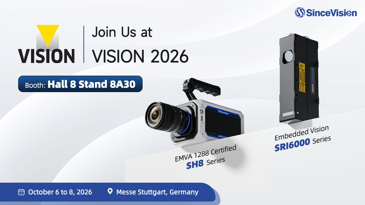
At VISION 2026 in Stuttgart, SinceVision Europe Sales Director Kevin Cheng will present practical engineering methodologies addressing both physical constraints across two technical forums: Industrial VISION Days, hosted by VDMA Machine Vision, and Scientific VISION Days, organized by the AIT Austrian Institute of Technology.
Part 1: Solving 3D Laser Triangulation Bottlenecks in AI Hardware Production
The rapid deployment of high-power AI server accelerators has redefined tolerance envelopes for core mechanical and electrical interfaces. High-density printed circuit boards, high-bandwidth memory (HBM) packages, and liquid cooling distribution plates require tighter geometric tolerances and accelerated inline verification.
Physical Inspection Challenges in AI Computing Hardware
- Specular Reflection and Multi-Path Interference: Liquid-cooled cold plates and heat spreaders combine milled copper or aluminum with nickel plating. Highly reflective curved surfaces, such as semicircular fluid injection ports, generate secondary and tertiary reflections that bounce off surrounding metal walls. Standard triangulation sensors misinterpret these secondary optical paths as elevated surface features, creating phantom artifacts and incorrect profile tolerances.
- Optical Boundary Shift Across Mixed Materials: High-performance processor boards pair high-reflectivity metallic interconnects directly adjacent to dark, light-absorbing epoxy resin fills. In conventional line laser profilers, the asymmetric optical absorption across this material boundary distorts the received light distribution, shifting the calculated peak center and causing false step errors.
- High-Speed Coplanarity Tolerances on Solder Arrays: Large-scale Ball Grid Array (BGA) packages feature dense arrays of mirrored solder balls. Detecting height variation across thousands of micro-spheres requires maintaining sub-10 micrometer measurement error while operating at production line velocities of 150 millimeters per second.

Engineering Solutions: Symmetrical Beam Optics and Spatial Filtering
To maintain data fidelity at 67 kHz profile rates, SinceVision implements optical and algorithmic compensation techniques within the SRI Series 3D laser profilers:
- Symmetrical Spot Profile Correction: The projection optics generate a strictly symmetrical laser distribution that preserves the true Gaussian center of mass across steep reflectivity steps, preventing false elevation steps at metal to resin interfaces.
- Algorithmic Elimination of Multi-Path Noise: Dynamic thresholding isolates the direct primary laser reflection from multi-bounce specular returns. This ensures accurate dimensional metrology on liquid cooling plates, verifying that thermal spreaders achieve flat, gap-free contact with GPU dies without requiring mechanical contact probes.
Part 2: Bridging Laboratory Sensitivity and Factory Floor Velocities with Cooled sCMOS
While 3D geometric profiling resolves macro-scale mechanical tolerances, front-end semiconductor, wafer, and advanced display quality control face an entirely different physical hurdle: single-photon signal recovery under microsecond exposure budgets.
The Trade-Off in High-End Industrial Optical Screening
Defects in advanced semiconductors, Micro-LED arrays, and thin-film photovoltaic wafers rarely manifest as clear physical contours. Instead, critical electrical anomalies and lattice stress fractures are detected via ultra-faint electroluminescence (EL) or photoluminescence (PL).
Historically, production facilities have balanced three imperfect inspection trade-offs:
- Increasing Illumination Intensity: High-intensity light risks inducing thermal shock or localized surface degradation in thin-film structures.
- Extending Exposure Times and Multi-Frame Averaging: Averaging multiple frames lowers visible background noise, but cycle times balloon from milliseconds to minutes, forcing automated production lines to revert to off-line batch sampling.
- Deploying Scientific Laboratory Cameras: Scientific-grade cameras deliver ultra-low read noise, but their rolling shutters and low frame rates cause severe geometric distortion and image blur when moving substrates exceed 100 millimeters per second.
Certified System Integrator Program
Set Yourself at the Forefront of the Global Vision Market
 Vision system integrators certified by A3 are acknowledged globally throughout the industry as an elite group of accomplished, highly skilled and trusted professionals. You’ll be able to leverage your certification to enhance your competitiveness and expand your opportunities.

Architectural Breakthrough: Industrial-Grade Cooled BSI sCMOS
To bridge this operational divide, SinceVision developed the Solis B0555 PRO, an industrial backside-illuminated (BSI) sCMOS camera that provides research-grade photon sensitivity at high inline cycle rates.
Key Technical Pillars
- Sub-Electron Readout Noise (0.29e- RMS): Reducing the sensor read noise beneath the single-electron boundary allows individual photons to be quantified above the thermal background. Wafer micro-cracks and junction leakage points are detected within a single frame, eliminating multi-frame averaging entirely.
- High-Speed Global Shutter at 240 fps: An electronic global shutter exposes all pixels simultaneously across the array. Defect screening operates cleanly at production speeds up to 500 millimeters per second without rolling-shutter spatial compression or edge tearing.
- Broad Spectral Response from DUV to NIR: High quantum efficiency across the ultraviolet (200 nm) and near-infrared (1,100 nm) spectra enables dual-purpose operation: deep UV illumination for nanoscale surface contamination, and 1,100 nm detection for silicon substrate transmission and electroluminescence.
- Thermoelectric Cooling (-30°C): Active two-stage Peltier cooling stabilizes dark current down to 0.002 electrons per pixel per second, preserving dynamic range during faint luminescence exposures.
Technical Session Overview at VISION 2026
Both technological frameworks will be detailed with live comparative production data, optical path diagrams, and real-world application benchmarks during the official VISION 2026 conference programs in Stuttgart, Germany.
Industrial VISION Days (Organized by VDMA Machine Vision)
- Topic: Laser Triangulation Solves New 3D Inspection Demands in AI Computing Era
- Speaker: Kevin Cheng, Europe Sales Director, SinceVision
- Date & Time: Thursday, 8 October 2026 | 15:40 to 16:00
- Location: Hall 8, Booth C70, Messe Stuttgart

Scientific VISION Days (Hosted by AIT Austrian Institute of Technology)
- Topic: A New Generation of Low-Light, High-Fidelity Imaging System for Industrial Inspection Challenges
- Speaker: Kevin Cheng, Europe Sales Director, SinceVision
- Date & Time: Tuesday, 6 October 2026 | Morning Session
- Location: Hall 8, Booth C50, Messe Stuttgart

Get Your Free Ticket to VISION 2026
Step 1: Go to this link https://www.messe-stuttgart.de/vision/en/tickets-opening-times/
Step 2: Use the code "SINCEVISION"

Factory floor automation requires closing the gap between laboratory optical precision and harsh industrial manufacturing throughput. The integration of high-frequency symmetrical laser triangulation and deep-cooled sub-electron sCMOS imaging provides machine vision system integrators and equipment builders with the quantitative data precision needed to secure yield integrity across modern AI hardware and semiconductor supply chains.

Shenzhen SinceVision Technology Co. Ltd.
SinceVision is a sensor technology manufacturer for 3D laser profilers, high-speed cameras, laser displacement sensors, sCMOS cameras, spectral confocal displacement sensors, full-spectrum sensors, and through-beam edge sensors.
Discover how Shenzhen SinceVision Technology Co. Ltd. can support your automation journey with their complete range of solutions and expertise.
Related Posts
In the Global Race to Build Better Batteries, SinceVision Tackles the Friction of the Factory Floor
SHENZHEN, China — Inside the sprawling gigafactories that power the transition to electric vehicles, the…
Capturing the Invisible: SinceVision Brings Extreme High Speed Imaging to PhotoMechanics Conference 2026
When transient events occur in a fraction of a millisecond, standard sensors miss the action…
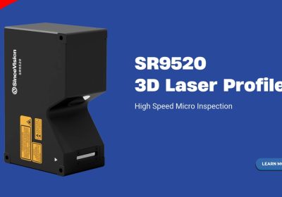
SinceVision’s New SR9520 3D Laser Profiler Brings 67kHz Micro Inspection to the Factory Floor
The push for denser lithium batteries, miniaturized 3C electronics, and tighter semiconductor packaging has created…
Leave a Reply